program/erase cycle (P/E cycle)

What is a program/erase cycle (P/E cycle)?
A solid-state storage program/erase cycle (P/E cycle) is a sequence of events in which data is written to a solid-state NAND flash memory cell, such as the type found in a flash or thumb drive, and is subsequently erased and rewritten.
The way that data is written and updated on a NAND flash device differs from how it is done on a hard disk drive (HDD). A flash solid-state drive (SSD) stores data in blocks, with each block separated into pages. A block might contain 64, 128 or 256 pages, with page sizes ranging between 4K and 16K.
NAND flash is unique because the storage controller writes and reads data at the page level but erases data at the block level. Additionally, data is written to empty pages. And data cannot be overwritten as is possible with an HDD.
For example, when a user modifies a file stored on a flash SSD, the updated data is written to empty pages, and the original pages are marked as invalid. Pages that contain invalid data cannot be reused until they are erased. To reclaim the invalid pages, the controller must move the pages with the valid data to another block. The original block can then be erased and used for new data.
A new flash SSD has empty pages, so writing data is a straightforward and efficient operation. As the drive fills up, the controller must move data and erase blocks before new data can be added. This process of erasing and writing (programming) data is referred to as the P/E cycle.
A flash memory device supports a limited number of P/E cycles because each cycle causes a small amount of physical damage to the individual data cells. This damage occurs when electrons pass through a thin oxide layer that separates the cell substrate from other cell components, such as a floating gate or charge trap layer. Repeated P/E cycles cause the oxide layer to degrade, which results in an increasing number of bit errors until a block is no longer usable.
How many P/E cycles does a flash SSD support?
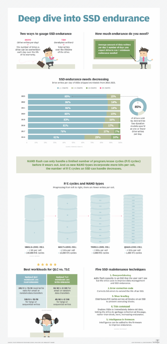
The maximum number of P/E cycles that a flash drive supports depends on the type of NAND cells, the size of the cells and the number of bits per cell.
Today, most NAND flash drives use either floating gate cells or charge trap cells. Until recently, floating gate cells dominated the SSD market, but with the advent of 3D NAND, charge trap cells have increased in popularity. While the two cell types are structurally similar, they differ in several ways:
- The floating gate is a conductor made up of polycrystalline silicon, and the charge trap is an insulator made up of silicon nitrate, which is less susceptible to defects and leakage.
- The charge trap cell uses a thinner oxide layer, making it possible to use less voltage to carry out P/E cycles. It also supports faster read/write operations and offers greater endurance.
- On the other hand, the charge trap cell tends to be susceptible to data degradation at high temperatures. When this occurs, it might not perform as well as the floating gate cell.
The number of supported P/E cycles can also be affected by the size of the cells. To create SSDs with greater capacities, storage vendors are shrinking the cell size to squeeze more cells onto each NAND chip. However, smaller cells can impact performance and lead to faster cell degradation, ultimately shortening the life span of the drive.
Storage vendors have also attempted to squeeze more bits into each cell, which can also affect the maximum number of P/E cycles that a drive can support. The following table provides an overview of the different types of NAND cells, based on the number of bits per cell.
| Cell type |
Bits per cell |
Supported P/E cycles |
| Single-level cell (SLC) |
1 |
100,000 |
| Multi-level cell (MLC) |
2 |
10,000 |
| Enterprise MLC (eMLC) |
2 |
30,000 |
| Triple-level cell (TLC) |
3 |
3,000 |
| Quad-level cell (QLC) |
4 |
1,000 |
| Penta-level cell (PLC) |
5 |
10 (still in research) |
The P/E cycle numbers listed in the table are cited throughout the storage industry, but in practice, these numbers can vary significantly. For example, inadequate wear leveling or environmental factors, such as high temperatures, can reduce the number of P/E cycles that a drive can support. Even if the totals are off, they still support an important aspect of cell density: The more bits per cell, the fewer supported P/E cycles.
See also: non-volatile memory, non-volatile memory express, SSD write cycle, read-intensive SSD, write endurance.